16V/70A DrMOS
![]()
- Parameters
- Features
- Description
| Part number | SY26670NGG |
|---|
| Vin (min) (V) | 5 |
|---|
| Vin (max) (V) | 16 |
|---|
| Vcc (V) | 3.3 |
|---|
| VDRV voltage (V) | 3.3 |
|---|
| Iout (max) (A) | 70 |
|---|
| IMON accuracy (±%) | 5 |
|---|
| Switching frequency (max)(kHz) | 200 |
|---|
| Switching frequency (min)(kHz) | 2000 |
|---|
| Features | Cycle-by-cycle current limit |
|---|
| Package | LGA5×6-41 |
|---|
| Operating temperature range(°C) | -40 to 125 |
|---|
| Functional safety category | |
|---|
- 70A Output Current Capability
- Integrated Driver, Power MOSFET and Decoupling Capacitors
- VDRV/VCC/BST/VIN UVLO
- Support Switching Frequency up to 2.0MHz
- 3.3V PWM Input Compatible with Tri-state Logic
- Integrated 5µA/A Current Sensing andAccurate Inductor Current Report
- Integrated 8mV/°C Temperature Monitor and Report
- Provide OTP with Fault Flag
- Cycle-by-cycle Peak Current Protection with Fault Flag and Negative Over Current Protection
- Programmable Threshold for Peak Current and Valley Current Protection
- Auto Refresh for VBST Power Supply in Tri�state
- Common Footprint Package: LGA5×6-41
Power Stage SY26670NGG is a monolithic power stage integrating a dedicated half bridge gate driver and both high side and low side MOSFETs to achieve high power density and high efficiency. Optimized switching edge, best in-class MOSFET and comprehensive protection logic make it suitable for CPU, GPU and POL power designs.
The SY26670NGG operates with VDRV/VCC from 3.0V to 3.6V and 3.3V PWM input signal, available for the switching frequency up to 2.0MHz. Tri-state PWM input is achieved for power-saving operation mode. Dead time and propagation delay time are optimized for high efficiency and reliable operation. Switching edge is tuned carefully for better efficiency and EMI performance. SY26670NGG provides low voltage spike and switching loss with embedded driving capacitor and input voltage capacitor.
The SY26670NGG integrates an on-chip temperature monitor to report the real-time junction temperature via TMON/FLT pin, this pin can also be pulled up or down as the fault flag together with IMON/FLT pin. The SY26670NGG provides a current reporting function via IMON/FLT pin, which achieves ±5% accuracy over temperature range. Cycle-by-cycle peak and valley current limit threshold can be programed by external resistor to protect the MOSFET.
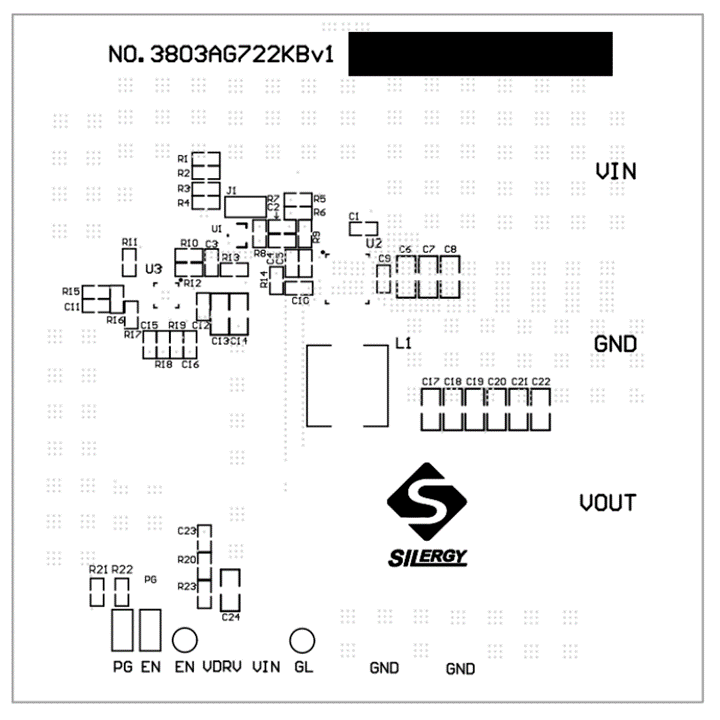
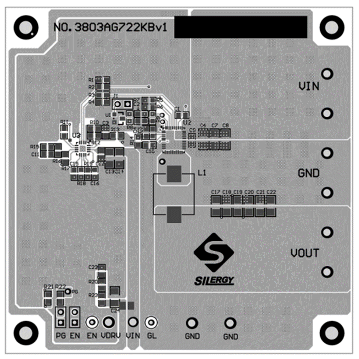
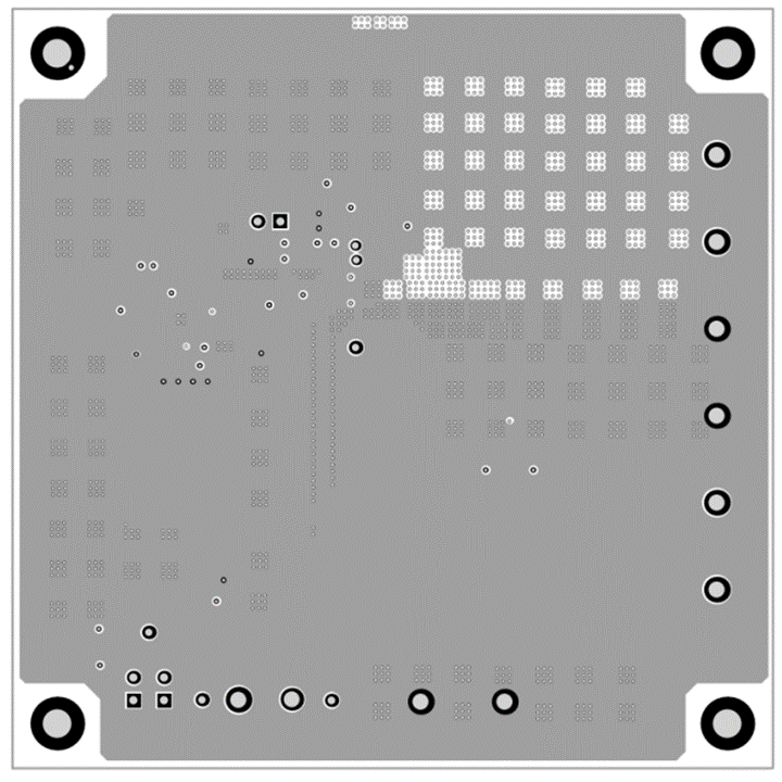
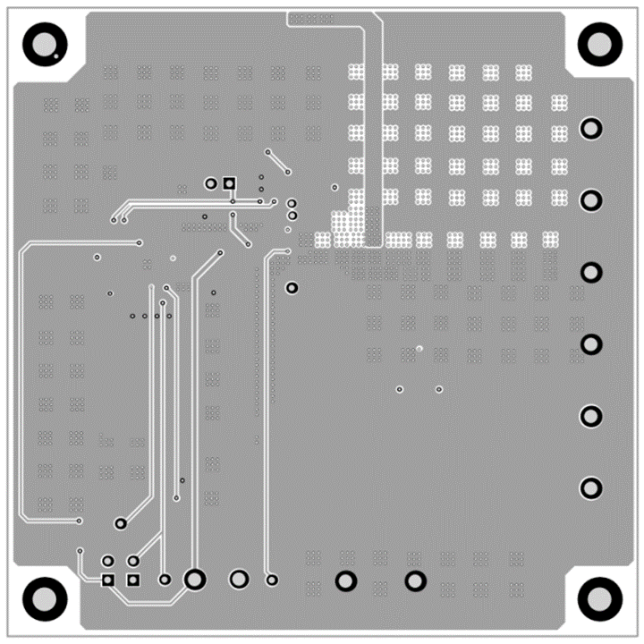
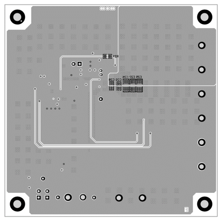
Evaluation Board
Photo of evaluation board
Photo of evaluation board
Photo of evaluation board
Photo of evaluation board
Photo of evaluation board
Photo of evaluation board
The EVB_SY26670NGG is intended for evaluating 500kHz, 70A DrMOS.